


Intel Ups Performance Ante With ‘Haswell’ Xeon E5 Chips
Any company that bought racks of servers within the past six months is probably going to be annoyed this week. The drumbeat of Moore's Law continues apace with the launch of the "Haswell" generation of Xeon E5-2600 processors, the third generation to bear that name and to provide a decent bump in both single-thread performance and a big jump in overall system throughput for the workhorse two-socket servers that dominate the datacenter. The Haswell Xeon E5s follow relatively fast on the heels of the "Ivy Bridge" Xeon E5-2600 v2 processors announced a year ago.
The interesting thing about this Haswell Xeon E5 launch is that it shows how Intel is not being driven so much by competition as it is by the increasingly diversifying needs of its customer base – both server makers and end users who commission their own machines from original design manufacturers and the needs of storage and networking gear makers, too.
There are 26 different versions of the Haswell Xeon E5 processors that are aimed at two-socket servers plus one for workstations and two more for single-socket machines, but even those lines are a bit fuzzy. The Haswell Xeon E5 aimed at workstations will probably find a home in overclocked servers (you cannot overclock the standard server-designated Xeons) and of course any of the Xeon E5s can be used in a two-socket workstation.
There is not just one Haswell Xeon E5 chip, but rather three different dies, and on top of this variety there are an unknown number of customized SKUs that large customers have commissioned. Some such customers gave paid Intel to added instructions that only they can access, or have made other kinds of modifications, such as deep bin searching to run them overclocked.
The diversity of feeds and speeds and prices with the Haswell Xeon E5s is both wider and deeper than with the prior Ivy Bridge Xeon E5 v2 chips bearing the 2600 designation. (The 2600 series Xeons are also known as the "efficient performance" or EP variant of the chip, to use Intel's internal language.) But there is a reason for this diversity.
As Eoin McConnell, Xeon E5 family product line manager, explained to EnterpriseTech at a pre-briefing in the chip maker's Oregon research facility, Intel has eliminated the Xeon E5-2400 EN series. For the past two generations, the EN chips were a variant of the EP parts that supported less memory, had fewer PCI-Express ports, only one QuickPath Interconnect (QPI) link between the sockets instead of two with the E5-2600s, and lower clock speeds. Consequently, the Xeon EN chips also had lower prices. The two different families used different sockets as well, which complicated things for motherboard and server makers. So with the Haswell Xeons, the 2400 and 2600 lines have been, for all practical purposes, converged. Now customers looking for a cheap chip do not have to make any sacrifices on I/O or memory.
It is not clear if Intel will be doing a four-socket variant of the Haswell-EP chips, which is akin to a poor man's Xeon E7-4800. McConnell was mum on the subject during our briefing. But it seems likely that we will see a Xeon E5-4600 v3 if there is demand for a system that does not need all of the bells and whistles of a Xeon E7-4800 machines and that costs a lot less, too.
Ticking And Tocking
Intel employs what it calls a "tick-tock" model in designing and manufacturing Xeon chips. The tocks are when a new microarchitecture is rolled out and the ticks are when that microarchitecture is tweaked a little bit and then implemented on a new manufacturing process that shrinks the transistors. In recent years, this shrinkage has allowed for more cores and L3 cache memory to be added to the die as well as other features. Haswell is technically a tock and its chips are implemented in the same 22 nanometer processes that were used with the Ivy Bridge Xeon E5 chips, a tick. The next tick comes with the "Broadwell" Xeons, which will move the Haswell architecture to 14 nanometer processes, followed by the tock of the "Skylake" Xeons, which will have a new microarchitecture implemented on the same 14 nanometer processes. Intel probably has room in its CMOS processes to keep ticking and tocking a few years into the next decade – and perhaps a little longer.
With the Haswell Xeon E5 chips, Intel is adding a bunch of goodies to the new cores to boost their performance for number-crunching and virtualization as well as cranking up the core count to increase the overall throughput per socket. As we pointed out above, there are actually three different Haswell Xeon E5 dies, and conceptually here is what the largest Ivy Bridge and Haswell Xeon E5-2600 chips look like:
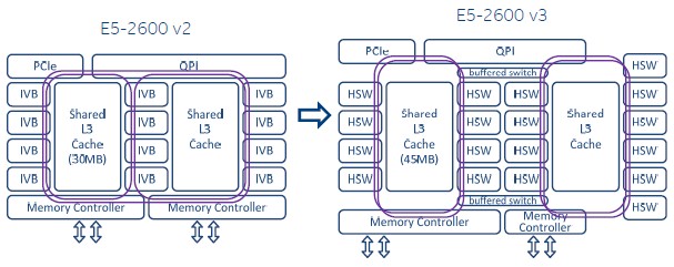
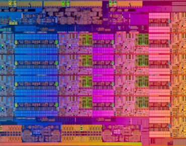
As you can see, the top-bin part in the E5-2600 v3 line has 18 cores, compared to 12 for the v2 chip, and the die shot at the top of this story shows what this 18-core Xeon E5 v3 beast really looks like. For fun, here is a block diagram of the three different Haswell Xeon E5 variants, which provides a conceptual layout of the different pieces of each chip. You best get out your reading glasses for this one:

The high core count, or HCC, variant of the Haswell Xeon E5 has from 14 to 18 cores and has two switch interconnects linking the rings that in turn lash together the cores and L3 cache segments together with the QPI buses, PCI-Express buses, and memory controllers that also hang off the rings. The HCC variants have 5.57 billion transistors and a die size of 31.93 millimeters by 20.72 millimeters (around 662 square millimeters); they have a thermal design point of between 110 watts and 145 watts.
The medium core count, or MCC, variant has from 10 to 12 cores and basically cuts off six cores and bends one of the rings back on itself to link to the second memory controller on the die. It weighs in at 3.84 billion transistors and has a die size of 24.01 millimeters by 20.15 millimeters (or around 492 square millimeters). The thermals for the MCC version range from 65 to 160 watts (the latter is for the official workstation part).
The low core count, or LCC, version of the Haswell Xeon has from 4 to 8 cores and is basically the left half of the MCC variant with the two interconnect switches, four of the cores, and the bent ring removed. This LCC chip has 2.6 billion transistors and has a die size of 17.57 millimeters by 20.15 millimeters, or around 354 square millimeters.
All three chips plug into a new variant of the LGA 2011 socket, also known as Socket R3, which has the same shape, size, and number of pins as the Socket R2 used for the Sandy Bridge and Ivy Bridge Xeon E5s but which uses the pins differently. Therefore the Haswell Xeons are not compatible with existing servers. The three different types of Haswell Xeon E5 dies are packaged up in versions that focus on core count, frequency, or low power and there are some that fall in the middle as well and have not been given a subcategory by Intel's marketing department. Here are how the different chips stack up and their prices:
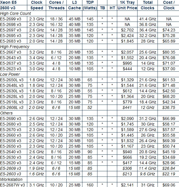
The two Haswell Xeon E5 chips with the highest core count, right at the top of this table, do not have list pricing, which is a bit peculiar and out of step with Intel's usual practices. When EnterpriseTech was briefed on these processors, pricing had not been set yet, so there was no reason to expect Intel to not provide a price for them.
When asked about why these two had no pricing, this is what an Intel spokesperson initially said in way of explanation. "It turns out we are not providing pricing for the 2699 v3 and 2698 v3 SKUs. Those are unique offerings that fall outside of our traditional, publically available 2S product offering. They were created in response to customer requests to design higher performance optimized SKUs, and to maximize awareness and adoption by increasing visibility to these SKUs." We then followed up and asked who the customers might be for these chips and received this further clarification: "The parts are being used across a broad range of customers looking for the maximum performance capabilities in a 2S configuration. The potential market usages include HPC, virtualization and cloud. These products are available directly to all customers. They are not customized SKUs only available for specific customers."
If there is a pattern to the chip pricing, and we are not suggesting there necessarily is, then the 18-core E5-2699 v3 should cost somewhere around $3,400 a pop and the 16-core E5-2698 v3 should cost around $3,000. (Intel's list pricing is for single units when bought at a 1,000-unit tray level. So we are talking millions of dollars per tray.)
Most of the Haswell Xeon E5 chips support Turbo Boost and HyperThreading, the former which allows for clock speeds to be jacked up if there is thermal room to do and the latter presenting two virtual threads per core to the operating system, which can increase throughput for a lot of workloads.
Given the wide variety of core counts, clock speeds, cache sizes, and differences in QPI speeds, it is hard to make generalizations across the Haswell Xeon E5 line and even more difficult to make any kinds of generalizations across product families. And yet, companies do have to choose processors somehow and there are no relative benchmarks that pin a performance metric to each SKU, and Intel does not provide similar data across product families. This would cut against the idea that everyone's performance varies and would be an explicit guarantee of performance as well, which Intel doesn't and perhaps should not make.
That said, you need some sort of relative performance proxy, and what I have always used since there were multicore processors is the aggregate clocks per core, and I divide this into the per-unit price to get a relative price/performance metric that spans each family. This is shown in the table above, and as you can see, Intel is charging a premium for chips with higher clock speeds and for higher core counts, which is exactly what you would expect because this is how it has always been in the computer business, whether you are talking about the capacity of a server, a memory module, or a disk drive. Price has never scaled linearly with capacity because at the upper end of any devices scalability limits the costs to bring that device to market is higher. It is fair to assume that Intel brings more money to the bottom line on these high core and high frequency variants, but there is no way to be sure.
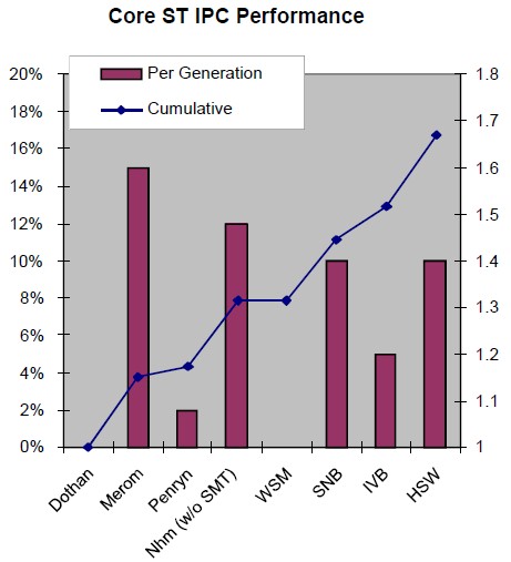
If you wanted to get clever about comparing across generations of Xeon chips, you could adjust the aggregate CPU oomph by the average instructions per clock (IPC) of each generation. Chris Gianos, the chip engineer who has been driving the development of the Haswell Xeon E5 for the past several years, provided this nifty chart that shows the IPC jumps for each generation of Intel cores way back to the "Dothan" Pentium M core from 2004. What this shows is that all of the tweaks and changes that Intel has done in the past decade to the Xeon cores have boosted the single-threaded instructions per clock performance by a factor of 1.7X. This is obviously important for single-threaded applications – like Intel's own electronic design automation software, for instance, that actually drives Moore's Law – and has become especially important as thermal limits have put a cap on clock speeds at around the 3.5 GHz range.
In general, the Haswell core delivers about 10 percent better IPC than the Ivy Bridge core, through a mix of better branch prediction, deeper buffers, larger translation lookaside buffers (TLBs), and a larger number of execution units. To feed the higher floating point capacity of the Haswell core, Intel has also doubled up the bandwidth on the L1 and L2 caches in each core. The Fused Multiply Add (FMA), AVX, and cryptographic elements of the Haswell core have also been significantly improved. (More on that in a moment.)
As has been the case for the past several generations of Xeon chips, there are customized versions of the Haswell Xeon E5 processors that selected customers have commissioned and that are not part of the lineup above. McConnell would not divulge what kinds of customizations these elite customers have asked for, or who such customers are, but he did confirm to EnterpriseTech that such customization is now part of the normal process of chip development at Intel.
"Our goal is to try to meet the majority of the market needs with the 29 SKUs that we have," explained McConnell. "Having 29 is a lot of SKUs, but if you look at the range we are trying to cover – everything from one socket workstations out to storage and comms – we feel we have a lot of the market covered, especially if you look at the range of cores, from 4 to 18, and different things we are varying with each SKU." That said, Intel will "entertain customer requests" for any modification to any of its processors, and has a set list of criteria by which those entertaining ideas turn into bespoke products. What those criteria are, McConnell obviously cannot say.
Let's Take A Look Under The Ceramic
The details of the Haswell cores have been known for nearly two years now, since they debuted in early 2013 for Intel's desktop processors at that time. But Gianos and his team at Intel add some features to the core each time they grab it from the desktop chip group to transform it into a Xeon server chip. Here are the big ones that matter to server shoppers:
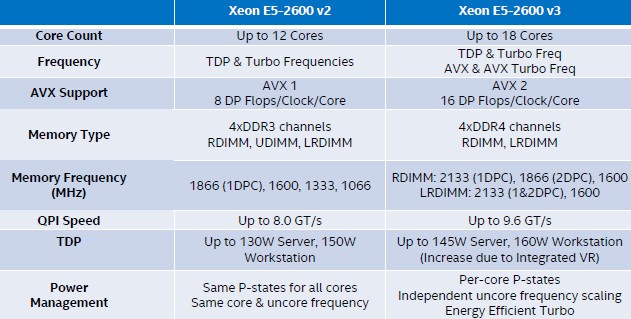
With the Haswell Xeon E5 chips, the top-end QPI speed has been increased by 20 percent to 9.6 GT/sec, providing the extra capacity to balance out the faster main memory and increased core counts per socket that come with these new chips. Processors with fewer cores have QPI ports that run at 8 GT/sec or 6.4 GT/sec and these also use lower memory speeds to keep things in balance.
As with the prior generations of Xeon E5 chips, the Haswell iteration allocates 2.5 MB of L3 cache per core, which is united into a single L3 cache by the rings and which is shared by all of the cores. As with most chip architectures today, there are sophisticated routines that help place data in the local cache segment where it is to be processed. In a very fractal way, this is akin to the non-uniform memory access (NUMA) algorithms that are used in servers with more than one processor. These routines are used to make sure data gets to the main memory closest to the socket where it will be processed. And in fact, there is a new feature called Cluster On Die, or COD, that breaks the Haswell Xeon E5 chips with 10 or more cores into different NUMA regions to make sure the data doesn't drift too far from the cores in these beasts. It essentially breaks the chip at the interconnect switch and treats it like two chips as far as the software is concerned, and for many workloads, this actually boosts performance significantly.
The wattages for the Haswell Xeon E5 chips probably look a bit higher than you expected, and there is a reason for this. That is because the processor now includes an integrated voltage regulator, a component that has, up until now, been external to the chip. (Memory controllers and PCI-Express controllers used to be outside the die on motherboards once, too.) This voltage regulator controls the voltage for CPU cores, system agents, and I/O controllers and provides a 1.8 volt rail for all non-memory voltage regulators in the system. (The memory controller has had its own power rail and voltage regulator since it was incorporated on the Xeon die many generations ago.) The Xeon chip can deliver whatever voltages it needs, as it scales power states up and down, and can do so more quickly.
The Haswell cores have a new related function called Per Core Power States, or PCPS, and it allows each core on the die to run at its own frequency and voltage combination. Intel has also tweaked the areas outside the core with a feature called Uncore Frequency Scaling, or UFS, which as the name suggests allows the components of the chip outside of the cores to scale their frequency up and down independently of the cores.
With the "Nehalem" and "Westmere" Xeons, the cores could Turbo Boost but the uncore regions stayed at a fixed frequency. With the Sandy Bridge and Ivy Bridge chips, the cores and uncore turboed up and down together. With Haswell and its Turbo Boost 2.0 features, the two elements of the chip can turbo up and down independently. That means applications that are bound by memory and cache latency can drive the uncore (the L3 cache and the interconnect rings) faster without boosting the cores; applications that are bound on compute can boost their core clocks without having to raise the uncore regions and wasting power. The feature that makes decisions about when to boost the cores and the uncore is called Energy Efficient Turbo, and is does the math to make sure a workload doesn't just crank the cores reflexively to try to get more work done when in fact what it needs to do is boost the uncore because the application is really waiting for data to come out of cache or main memory.
The Turbo Boost 2.0 toolbox also includes a feature called Turbo State Limiting, which puts a cap on the turbo states on the cores to cut down on the variability of clock frequencies. This is important for both high frequency trading and high performance computing workloads where, as Gianos put it, companies "know their applications swing but they do not want their processors to" because this messes with the overall performance of the application. In clusters, having software running consistently across nodes and networks is often more important than having each node or core going as fast as it can on each piece of work.
Another change with Turbo Boost 2.0 is that the AVX vector units and the cores now have their own base and turbo frequencies.
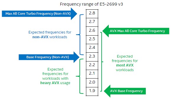
The reason is that workloads that heavily use the AVX math units tend to make the chip run a little hotter, so you have to back off the clocks a little to make the thermals all work out. The AVX units in the prior Ivy Bridge chips had 256-bit widths for floating point operations and 128-bits for integers, but with AVX2 in the Haswell chips, both integer and floating point registers are 256-bits wide. The AVX unit could do 8 double precision floating point operations per clock per core in Ivy Bridge Xeons, and the AVX2 doubles that up to 16 DP flops per clock per core with the Haswell Xeons.
Taking It All For Grantley
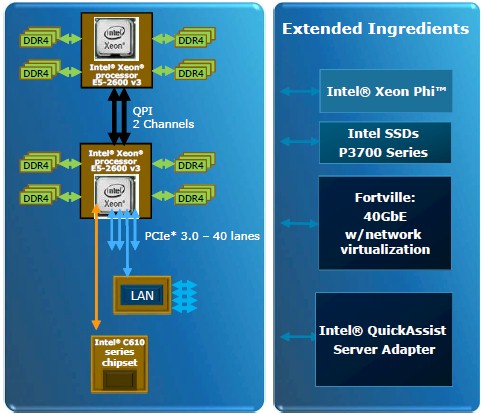
Stepping out of the processor and into the Haswell platform, which is code-named "Grantley," Intel is getting out in front of the DDR4 memory wave much as it got out in front with PCI-Express 3.0 peripherals with the Sandy Bridge chips.
Intel is the first chip maker to roll out support for DDR4 memory, which is being manufactured for servers by Samsung Electronics, Micron Technology, SK Hynix, and Elpida at the moment. The interesting thing is that servers usually lag desktops in the adoption of memory chip technology, but this time around, because of lower power and higher bandwidth needs, servers are getting out ahead of PCs with the latest main memory.
"We are going to drive the transition to DDR4 memory and we are pretty excited about it," explained McConnell. The Haswell Xeon E5 socket has four memory channels and supports two memory sticks per channel when the memory is running at 1.33 GHz, 1.6 GHz, or 1.8 GHz. But if you boost it up to 2.13 GHz, Intel is only supporting one stick per channel. McConnell said that server makers might certify two sticks per channel at that higher 2.13 GHz speed, but that Intel was only recommending one stick at the moment. He did not elaborate as to why, but it could be a bandwidth issue across the two QPI ports that link the sockets together.
We will dive into the benefits of DDR4 memory for Haswell servers in a separate story, but generally speaking, DDR4 memory sticks run at 1.2 volts compared to 1.5 volts for regular DDR3 sticks and burn about 2 watts less energy per stick. On the STREAM memory benchmark tests, the bandwidth using DDR4 was about 14 percent higher for a Haswell machine compared to a similarly configured Ivy Bridge machine using DDR3 memory. In some cases, memory bandwidth and the power efficiency of the DDR4 memory will be as much as 50 percent higher than for DDR3, Intel says.
The Haswell Xeon E5 chips have the same 40 PCI-Express 3.0 lanes linking to on-chip controllers, and the processors plug into the "Wellsburg" C610 chipset, which has four lanes of DMI2 into the processor and then support for up to ten SATA3 ports, eight USB2 ports, six USB3 ports, and one Gigabit Ethernet port coming out the other side of the chipset.
Intel is putting the finishing touches on its benchmark results, but says that in preliminary tests pitting a 12-core Xeon E5-2697 v2 against an 18-core E5-2699 v3, software makers are seeing anywhere from 20 to 90 percent improvement. Floating point performance can be as high as 2X thanks to the doubling of flops per clock per core and the 50 percent increase in the cores, using the Linpack test as a guide. The mileage on real applications varies depending on the sensitivity of the workload to frequency, core count, and features such as AVX2 vector math units. We will dig into the details once the final benchmark results are made available.


