


NVIDIA Unleashes Monster Pascal GPU Card at GTC16
NVIDIA revealed its first Pascal-architecture based GPU card, the P100, at the seventh-annual GPU Technology Conference (GTC) in San Jose.Calling it “the most advanced accelerator ever built,” the P100 is based on the NVIDIA Pascal GP100 GPU — a successor to the Kepler GK110/210 — and is aimed squarely at HPC, technical computing and deep learning workloads.
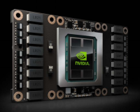
Packing a whopping 5.3 teraflops of double-precision floating point performance, the P100 is NVIDIA’s most performant chip to date. And with 15.3 billion transistors, it’s also the largest GPU that NVIDIA (NASDAQ: NVDA) has ever made, in spite of being built on TSMC’s 16nm FinFET manufacturing process.
The P100 is the flagship Pascal architecture offering, and it’s also the first product to implement the heralded HBM2 and NVLink technologies. During his keynote address, NVIDIA CEO Jen-Hsun Huang said the chip had entered volume production and would ship by first quarter 2017. Partners Dell, HPE, Cray and IBM are expected to come out with Pascal-equipped servers by the end of 2016, with production availability in early 2017.
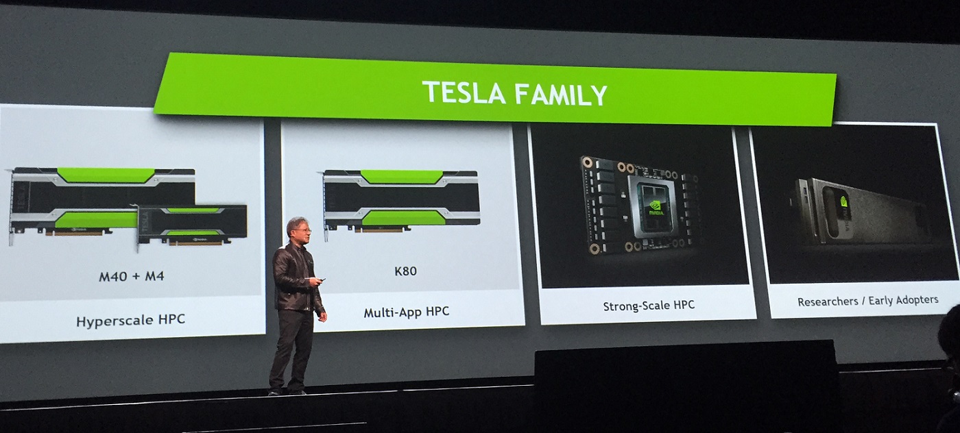
Huang also showed how the new Pascal GPU fits in with the Tesla family. The new DGX-1 deep learning supercomputer is shown all the way to the right. With a price tag of $129,000 the DGX-1 puts the equivalent of 250 servers in a box, said Huang. It packs eight of the new P100 GPUs and 7 TB of SSD storage and can pump out up to 170 teraflops of half-precision floating point performance. NVIDIA reported that the DGX-1 isn’t intended for clustering, although you never know what creative end users will try.
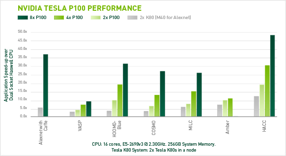
In a separate presentation, Lars Nyland, NVIDIA senior architect, and Mark Harris, chief technologist of GPU computing software at NVIDIA, provided a deep dive into the new architecture. Before unpacking the new features and specs, the duo looked at some real-world performance speedups for the P100. This chart depicts the benefits of the faster GPU and the high-bandwidth NVLink interconnect technology.
 GPU Breakdown
The cradle for computation in Tesla GPUs is the SM, the streaming multiprocessor. The SM creates, manages, schedules and executes instructions from many threads in parallel. The Tesla GP100 GPU has 60 SMs. For the P100, NVIDIA has enabled 56 of them for a total of 3,584 CUDA (enabled) cores. Memory bandwidth is 720 GB/s and the memory size is 16 GB.
There are 64 CUDA cores in the GP100 SM, which at first seems small in comparison to Maxwell’s SM with 128, but there is a reason. To arrive at the GP100 SM, NVIDIA started with a Maxwell SM and chopped it in half.
“The cores are your most important resource on the SM and if you don’t use them in any particular clock cycle, you are wasting your chip,” explained Nyland. “What we wanted to do was improve the efficiency to make them be used more often. We started with the Maxwell SM and we cut it in half – that gives us two P100 SMs. We could have stopped here, but we added the 64-bit floating point double precision cores and then we doubled the occupancy, we doubled the number of warps per P100 SM so that the occupancy went back to being equivalent to Maxwell SM. Then we also doubled the register files and finally we duplicated the shared memory – so now we have two SMs with 64 cores each from what we started with, one Maxwell 128 core SM.”
 The net effect, the NVIDIA reps go on to explain, is that the GP100 SM has more resources per core. It has twice the number of registers more core, 1.33x more shared memory capacity, 2x shared memory bandwidth and twice as many warps resident at the same time on the SMs.
The overall impact is higher instruction throughput leading to higher utilization when running codes. “There’s a big effort that’s gone into making sure you get more value out of every core,” said Harris.
“We’ve put more resources around each core” Nyland added, “By having more warps ready, the scheduler has more to choose from and so it has more opportunities to run something than it would if there were fewer warps. By having more register, we can have higher occupancy. And then having a shared memory, we have double the bandwidth and less contention, less cores shared with the shared memory so there is more access. All of this adds up to more utilization of the cores, which is the real goal.”
Floating point is cited as another critical resource. The three sizes – half-precision, single-precision and double-precision — all fit the IEEE standard. The peak speed of 5.2 teraflops double-precision performance doubles to 10.6 teraflops running in single-precision floating point mode. Double it again, and you get 21 peak teraflops of half-precision floating point performance — another first.
“GPUs have used half-precision for at least a dozen years as a storage mechanism to save space — for textures — but we’ve never built an arithmetic pipeline to implement the 16-bit floating point directly, we’ve always converted it,” Nyland said. “What we’ve done is left it in its native size and then pair it together and execute an instruction on a pair of values every clock – this is compared to the single-precision where we execute one instruction every clock and the double-precision runs at one every two clocks.”
NVIDIA has also added atomic addition for 64-bit floating point values.

NVLink
One of the most important new features that debuted with the Pascal architecture is NVLink, NVIDIA’s communications protocol that allows high-speed communication from one GPU to another and to future NVLink-enabled CPUs as well. The point-to-point interconnect is said to allow data sharing at rates five to 12 times faster than traditional PCI Express Gen 3 (PCIe). And its compatibility with the GPU ISA means it can support shared memory multiprocessing workloads.
Currently implemented in Tesla P100 accelerator boards and Pascal GP100 GPUs, NVLink supports reads, writes and atomics between GPUs. There are four NVLinks on every P100 GPU. A single link supports up to 40 GB/sec of bidirectional bandwidth between the endpoints and links can be connected in a gang to enable an aggregate maximum theoretical bandwidth of 160 GB/sec bidirectional bandwidth per P100. The ability to have four or eight GPUs all sharing data with each other is the real benefit of NVlink, said Harris. “We can build really powerful machines and still program them with familiar programming models,” he added.
 NVLink can also be coupled with an NVLink enabled CPU, like the future POWER CPU that IBM has announced. In this configuration, four P100 GPUs can be fully connected in a gang and they’ll have a link that connects to the CPU. The GPUs will thus be able to access all the memory of the other GPUs and CPU memory.
High Bandwidth Memory 2
The other major first for P100 is its use of HBM2 stacked memory. This technology enables multiple layers of DRAM components to be integrated vertically on the package along with the GPU. The P100 accelerators have four 4-die HBM2 stacks, for a total of 16 GB of memory, and 720 GB/s peak bandwidth.
With HBM2, error correcting code (ECC) functionality is free, the NVIDIA reps noted. What this means is there is no capacity taken away and there’s no processing performance penalty associated with using ECC. This wasn’t the case with the GDDR memories. For those, NVIDIA implemented an ECC scheme that used some of the memory for the ECC bit data and they had to create that data themselves, which had a slight penalty.
Unified Memory
Pascal has also expanded on the unified memory features of CUDA 6 by adding support for large address spaces and page faulting capability. Because Kepler and Maxwell weren’t allowed to page fault, the developer was only allowed to allocate unified memory up to the size of the GPU’s physical memory. Also, because the GPU can page fault, when you launch a kernel, any pages that were migrated to the CPU need to be migrated back to the GPU before the kernel can run – this translates to launch overhead. This meant that on Kepler and Maxwell the CPU and GPU code could not simultaneously access the same memory allocations.
“With the page migration engine, the larger address space and the ability to page fault, you now get all of these things you couldn’t do before,” explained Nyland. “You can allocate beyond the size of the GPU memory up to the physical system memory size, which means you can oversubscribe the GPU memory and do the processing of large scale models out of core. You can now simultaneously access those allocations from the CPU and GPU without fatal errors. This means you have much finer-grained communication between the processors but you do still have to take care of proper synchronization so you don’t have race conditions. You can even do unified memory atomic operations, and across NVLink these are native.”
In the future, on systems that support it, Pascal enables the possibility of using the system allocator to allocate unified memory. In this case, malloc would be able to pass those pointers to CPU or GPU and share that data. NVIDIA is working with Red Hat and the Linux community on the operating system changes that are necessary to unlock this functionality, reported Nyland.
More to come…
This was the first major walk-through of the Pascal architecture and GPU launch, however that’s by no means all of it. NVIDIA will be discussing other GP100 features — such as preemption and a larger L2 cache — in the days and weeks to come. A white paper is said to be forthcoming and we will link to it here when it’s available. For now, if you are hungry for more Pascal information, check out this blog post by Mark Harris, which reprises the content of today’s deep dive session.
Pricing for the Tesla P100 is not yet available and shipping is still about a year away, but there is a way to get your hands on one. The GPUs are available for $16,125 each in quantities of eight — if you spring for the DGX-1. NVIDIA also makes select hardware available to its joint lab partners and its early access program partners.


