


First Xeon-FPGA Integration Launched by Intel
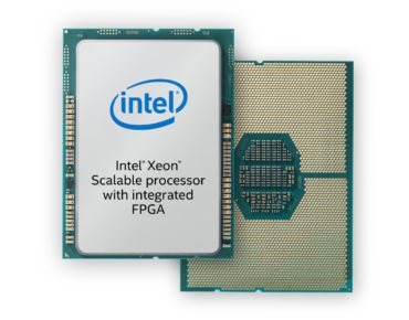
Intel’s Xeon Scalable 6138P with Intel Arria 10 GX 1150 FPGA
Ever since Intel’s acquisition of FPGA specialist Altera in 2015 for $16.7 billion, it’s been widely acknowledged that some day, Intel would release a processor that integrates its mainstream Xeon CPU server chip with lightning-fast FPGAs.
That day has arrived.
Available now for “select” customers, Intel’s Xeon Scalable 6138P processor with integrated Intel Arria 10 GX 1150 FPGAs marks the first production CPU with a coherently interfaced FPGA, according to industry observers.
Intel said the chip provides up to 160Gbps of I/O bandwidth per socket and a tightly coupled cache-coherent interface. The Arria FPGA portion of the processor has its own cache and shares memory with the CPU via cache coherent access over the Intel Ultra Path Interconnect bus, which Intel said allows seamless access to data regardless of where the data resides (core cache, FPGA cache, or memory) without the need for redundant data storage and direct memory access transfers. “Data coherency also reduces application programming complexity and saves CPU cycles that would be wasted to determine which data is most-up-to-date,” said Jennifer Huffstetler, Intel’s VP/GM of data center product management in a blog announcing the product.
Patrick Moorhead, president and principal analyst of industry watcher Moor Insights & Strategy, told EnterpriseTech the new chip “is the next step forward into bringing FPGAs deeper into the enterprise and therefore more mainstream.”
![]() “This should simplify workload sharing between CPU and FPGA,” Moorhead said, “as they share a coherent interface to memory, meaning the programmer should have an easier time writing accelerated applications. With coherency, the programmer has to worry less about mapping, copying and pasting data between on-board FPGA memory and system memory. This integration should also help with density and should enable more CPU+FPGAs compute per square meter and likely lower power draw.”
“This should simplify workload sharing between CPU and FPGA,” Moorhead said, “as they share a coherent interface to memory, meaning the programmer should have an easier time writing accelerated applications. With coherency, the programmer has to worry less about mapping, copying and pasting data between on-board FPGA memory and system memory. This integration should also help with density and should enable more CPU+FPGAs compute per square meter and likely lower power draw.”
Huffstetler noted the new chip includes Intel’s new virtual switching reference design, which uses the FPGA for infrastructure dataplane switching while the processor does application processing or processes virtual machines. “The combination helps simplify network complexity and improve the productivity of the processor,” she said.
This solution is also compatible with the Open Virtual Switch (OVS) framework and delivers a 3.2X throughput improvement at half the latency and 2X more VMs as compared to OVS running on an equivalent processor without FPGA acceleration, Huffstetler said. She added that code compatibility with Intel’s OVS-DPDK software eases data center retrofits while simplifying scalability for “operational agility.”
Fujitsu announced plans to deliver systems based on the Xeon processor with integrated FPGA and OVS reference design. “They are making the Intel virtual switching reference design even more robust for the networking environment through their reliability, availability, and serviceability with performance monitoring and debug assisting functions,” Huffstetler said.
She said Intel’s roadmap includes a discrete FPGA solution with faster coherent and increased bandwidth interconnect enabled by the Acceleration Stack for Intel Xeon CPU with FPGAs. “It will support code migration from the Intel Xeon Scalable processor with Integrated FPGA and the Intel Programmable Acceleration Card (Intel PAC) solutions, and will continue to be optimized for enhanced bandwidth and low latency,” Huffstetler said.


